Your shopping cart is currently empty.
DDESP-FM-V2
Geometry
RectangularTip Radius (nm)
Nom: 100
Max: 150
Frequency (KHz)
Nom: 105
Min: 80
Max: 130
Length (µm)
Nom: 225
Min: 215
Max: 235
Spring Const (N/m)
Nom: 6
Min: 3
Max: 12
Width (µm)
Nom: 35
Min: 33
Max: 37
Order a free DDESP-FM-V2 sample
Please note that we are only able to offer samples for shipping addresses within the United States of America.
Price: $1,470.00 (USD)
Sold in packs of 10
Questions? Free, Online Consulting
Overview
Bruker's popular DDESP-FM-V2 electrical probe provide both fantastic wear resistance and robust conductivity due to the hard and highly conductive tip side doped diamond coating.
Perfect for applications such as C-AFM and PeakForce TUNA, SCM, SSRM, and PFM.
For a stiffer cantilever version of this probe see DDESP-V2.
Probe part numbers ending in -V2 provide:
Tighter dimensional specifications for improved probe to probe consistency
More precise alignment of the tip to the cantilever apex
Improved aesthetics
Tip Specification
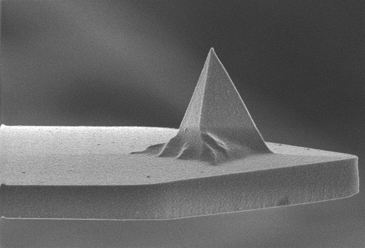
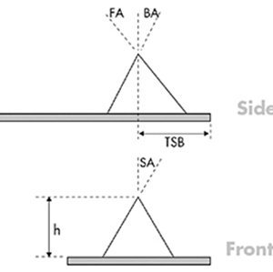
Tip Height (h): 10 - 15 µm
Front Angle (FA): 25 ± 2.5º
Back Angle (BA): 17.5 ± 2.5º
Side Angle (SA): 20 ± 2.5º
Cantilever Specification
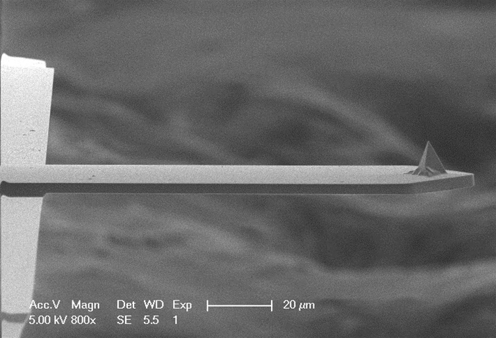
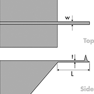
Material: 0.010-0.025 Ωcm Antimony (n) doped Si
Geometry: Rectangular
Cantilevers Number: 1
Cantilever Thickness (Nom): 2.95µm
Cantilever Thickness (RNG): 2.20 - 3.70µm
Back Side Coating: Reflective Aluminum