Your shopping cart is currently empty.
DDLTESP-V2
Geometry
RectangularTip Radius (nm)
Nom: 100
Max: 150
Frequency (KHz)
Nom: 280
Min: 190
Max: 380
Length (µm)
Nom: 225
Min: 215
Max: 235
Spring Const (N/m)
Nom: 95
Min: 45
Max: 190
Width (µm)
Nom: 40
Min: 38
Max: 42
Price: $1,470.00 (USD)
Sold in packs of 10
Questions? Free, Online Consulting
Overview
Bruker’s new series of conductive diamond coated probes provide consistent performance with high wear resistance in mechanical and electrical applications. In mechanical applications, these probes provide extreme wear resistance.
In electrical applications, these probes provide high performance in Scanning Spreading Resistance Microscopy (SSRM) and Piezoresponse Force Microscopy (PFM) to characterize advanced semiconductor devices, Microelectromechanical Systems (MEMS), and biosensors providing the prolonged tip lifetime in combination with boosted conductivity.
The DDLTESP-V2 probe provides:
• High performance contact resonance imaging with Dimension Icon
• High electrical performance due to its consistent tip shape
• Sensitive nanoelectrical measurements with highly conductive coating
• High resolution electrical imaging with a sharp conductive tip
• High quality probe manufactured by Bruker AFM Probes
• High spring constant for contact resonance on hardest materials such s ceramics
Other applications of this probe include: Scanning Capacitance Microscopy (SCM), conductivity measurements (C-AFM and PeakForce TUNA), and other electrical characterization applications.
Tip Specification
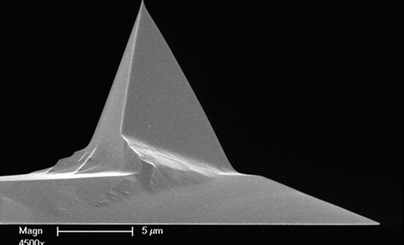
Tip Height (h): 10-15 µm
Front Angle (FA): 25+/-2º
Back Angle (BA): 15+/-2º
Side Angle (SA): 17.5+/-2º
Cantilever Specification
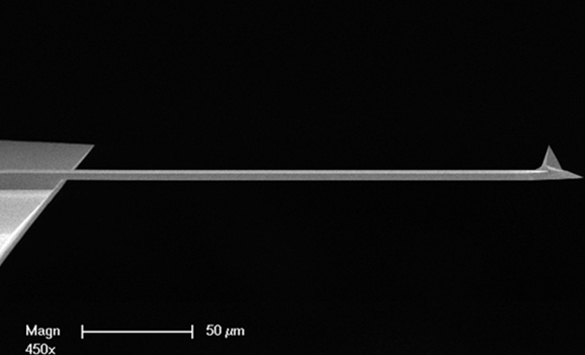

Geometry: Rectangular
Cantilevers Number: 1
Cantilever Thickness (Nom): 7µm
Cantilever Thickness (RNG): 6-8µm
Back Side Coating: Reflective Aluminum