Your shopping cart is currently empty.
SCM-PTSI
Geometry
RectangularTip Radius (nm)
Nom: 15
Max: 20
Frequency (KHz)
Nom: 75
Min: 50
Max: 100
Length (µm)
Nom: 225
Min: 200
Max: 250
Spring Const (N/m)
Nom: 2.8
Min: 1
Max: 5
Width (µm)
Nom: 28
Min: 23
Max: 33
Order a free SCM-PTSI sample
Price: $1,680.00 (USD)
Sold in packs of 10
Questions? Free, Online Consulting
Overview
For the highest resolution nanoelectrical measurements with outstanding wear resistance.
Bruker's platinum silicide AFM probe is the ideal choice for Scanning Capacitance Microscopy measurements, conductivity measurements (Conductive AFM (C-AFM) and PeakForce TUNA), Electrical Force Microscopy (EFM), and other characterization applications. on the most advanced semiconductor features, providing the highest resolution imaging and long tip lifetime due to its outstanding wear resistant properties.
Bruker's platinum silicide AFM probe is the ideal choice for Scanning Capacitance Microscopy measurements, conductivity measurements (Conductive AFM (C-AFM) and PeakForce TUNA), Electrical Force Microscopy (EFM), and other characterization applications. on the most advanced semiconductor features, providing the highest resolution imaging and long tip lifetime due to its outstanding wear resistant properties.
The Bruker SCM-PtSi probe provides:
• High resolution electrical imaging with an ultra-sharp conductive tip
• Consistent performance with high measurement lifetime
• Highly sensitive nanoelectrical measurements
Bruker Atomic Force Microscopy group also provides many other nano-electrical probes and modes for AFM based electrical measurements including our unique PeakForce KPFM & PeakForce TUNA modes.
Tip Specification
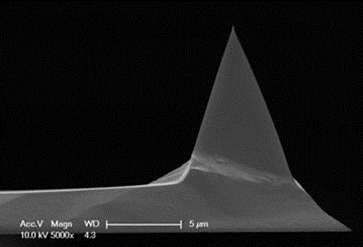
Tip Height (h): 10 - 15 µm
Front Angle (FA): 25 ± 2.5º
Back Angle (BA): 17.5 ± 2.5º
Side Angle (SA): 20 ± 2.5º
Cantilever Specification
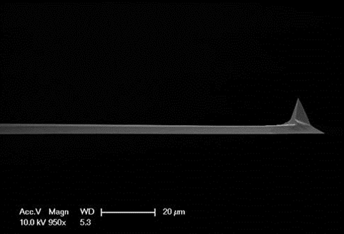

Material: 0.01 - 0.025 Ocm Antimony (n) doped Si
Geometry: Rectangular
Cantilevers Number: 1
Cantilever Thickness (Nom): 2.75µm
Cantilever Thickness (RNG): 2.0 - 3.5µm
Back Side Coating: Reflective Al