DDESP-V2
Geometry
RectangularTip Radius (nm)
Nom: 100
Max: 150
Frequency (KHz)
Nom: 450
Min: 300
Max: 600
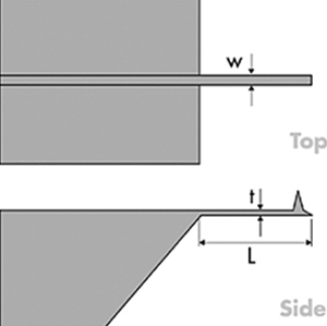
Length (µm)
Nom: 125
Min: 115
Max: 135
Spring Const (N/m)
Nom: 80
Min: 30
Max: 180
Width (µm)
Nom: 40
Min: 38
Max: 42
Order a free DDESP-V2 sample
Price: $1,400.00 (USD)
Sold in packs of 10
Questions? Free, Online Consulting
Overview
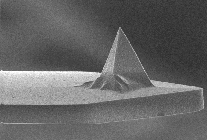
Bruker's popular DDESP-V2 electrical probe provide both fantastic wear resistance and robust conductivity due to the hard and highly conductive tip side doped diamond coating.
Perfect for applications such as C-AFM and PeakForce TUNA, SCM, SSRM, and PFM.
For a softer cantilever version of this probe see DDESP-FM-V2
Probe part numbers ending in -V2 provide:
Tighter dimensional specifications for improved probe to probe consistency
More precise alignment of the tip to the cantilever apex
Improved aesthetics
Tip Specification
The doped diamond coating is used to harden the tip in applications that require both increased wear resistance and a conductive tip. The tradeoff for the increased lifetime is that the coating also increases the diameter of the tip. If a conductive coating is not needed, the DLC coated probes (Model# TESPD) provide a cost effective alternative.
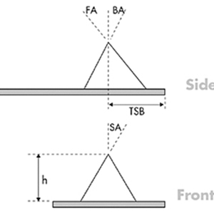
Tip Height (h): 10 - 15 µm
Front Angle (FA): 25 ± 2.5º
Back Angle (BA): 17.5 ± 2.5º
Side Angle (SA): 20 ± 2.5º
Cantilever Specification
Material: 0.010-0.025 Ωcm Antimony (n) doped Si
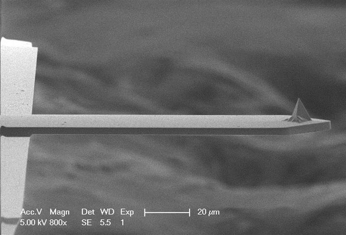
Geometry: Rectangular
Cantilevers Number: 1
Cantilever Thickness (Nom): 3.6µm
Cantilever Thickness (RNG): 2.85 - 4.35µm
Back Side Coating: Reflective Aluminum


